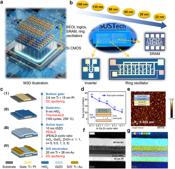
How can useful electronic devices be fabricated above completed CMOS? I am exploring low-temperature processing, materials selection, and the relationship between process history and device behavior.
A low thermal budget is a constraint on the whole process flow, not only the deposition temperature. Film quality, dielectric interfaces and subsequent treatment must be considered together. ALD and CVD offer different ways to control thin-film growth; the central question is how that control translates into a useful transistor while preserving the circuitry underneath.
My current interests include oxide semiconductors and emerging p-type materials, with particular attention to defects, contacts, threshold-voltage stability, and the opportunities for complementary electronics.
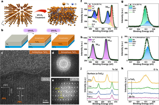
Complementary electronics brings the p-type channel into focus alongside established n-type oxide devices. Channel transport is only part of the challenge: carrier injection, dielectric interfaces and stability also shape circuit behavior. The literature figure illustrates one material route, amorphous tellurium trioxide, within this broader exploration of p-type oxides and complementary structures.
I am interested in complementary device structures and sequential integration of active layers, bringing device physics together with practical fabrication constraints. ALD, CVD, and related thin-film processes form part of the fabrication routes I am exploring.
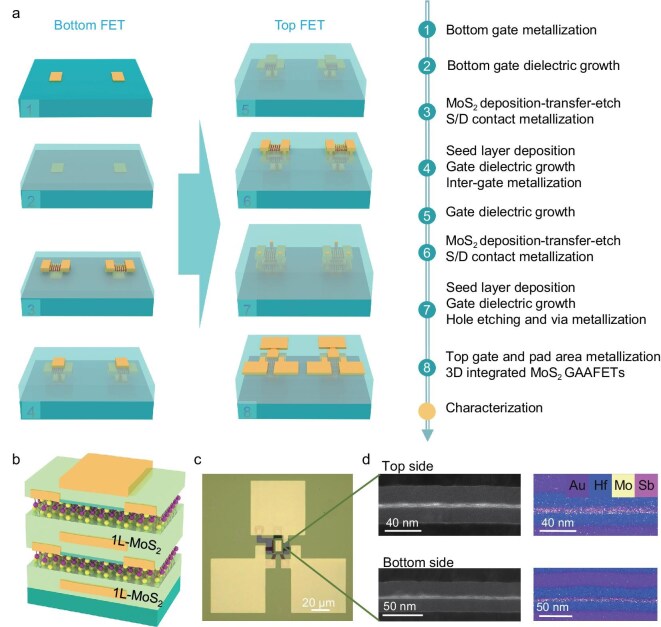
Sequential integration links the upper-layer device process to the layers already in place. Thermal exposure, layer-to-layer connections and gate-stack choices therefore become coupled design questions. The example shown uses MoS2 gate-all-around transistors to make this vertical architecture concrete; it helps frame the integration challenges that also motivate work on low-temperature semiconductor devices.
How I approach research
From physical mechanisms to integration choices.
I am drawn to questions where materials, process history, defects, and interfaces determine device behavior. My integrated-circuit background informs an interest in how those device-level choices translate into circuit function and manufacturable systems.
Materials → Process → Interfaces → Devices → Integration
Earlier foundations
My earlier work spans nano-TSV optimization, advanced-packaging simulation, semiconductor sensing, nanophotonics, and wafer inspection. These experiences connect computational methods with physical devices and engineering implementation.